Light at the Edge of Compute: Photonics and the Future of Data Infrastructure
This article is derived from a recent white paper authored by Pangaea Partner Andrew Haughian, available to Pangaea Strategic Limited Partners.
Why Photonics Is Moving Center Stage
The semiconductor industry is running into hard physical limits on how far traditional electronic interconnects can be pushed, just as AI and data-intensive workloads demand more bandwidth, lower latency, and greater energy efficiency. Inference now dominates many data centers, with massive numbers of concurrent, latency-sensitive requests that strain legacy networking architectures.
Photonic networking offers a way around these bottlenecks by moving more of the data path into the optical domain, where light can carry far more information with lower loss than copper. This shift is not just another speed bump on a roadmap, it is part of a broader hard tech revolution in compute and networking infrastructure, where materials innovation and systems-level design are reshaping what is possible in AI-era data centers.
Photonic Networking: Where the Shift Starts
Light has long been used to move data over long distances, but the requirements are changing as bandwidth needs grow inside and between data centers. A handful of core components do most of the work:
Transceivers convert electrical signals to light and back again and represent a large, fast-growing market that could exceed $30 billion by 2030.
Amplifiers boost optical signals without converting them to electrical form, but today are still too bulky and expensive for dense data center deployment.
Optical switches and interconnects route and carry light directly, with the potential to cut latency and power by avoiding repeated electrical conversions.
The technical challenges are clear. Transceivers must handle 800G+ and beyond while reducing power and managing heat. Amplifiers need to shrink and move closer to chips. Switches must move from microsecond to nanosecond-scale reconfiguration to support dynamic, packet-level routing for AI workloads.
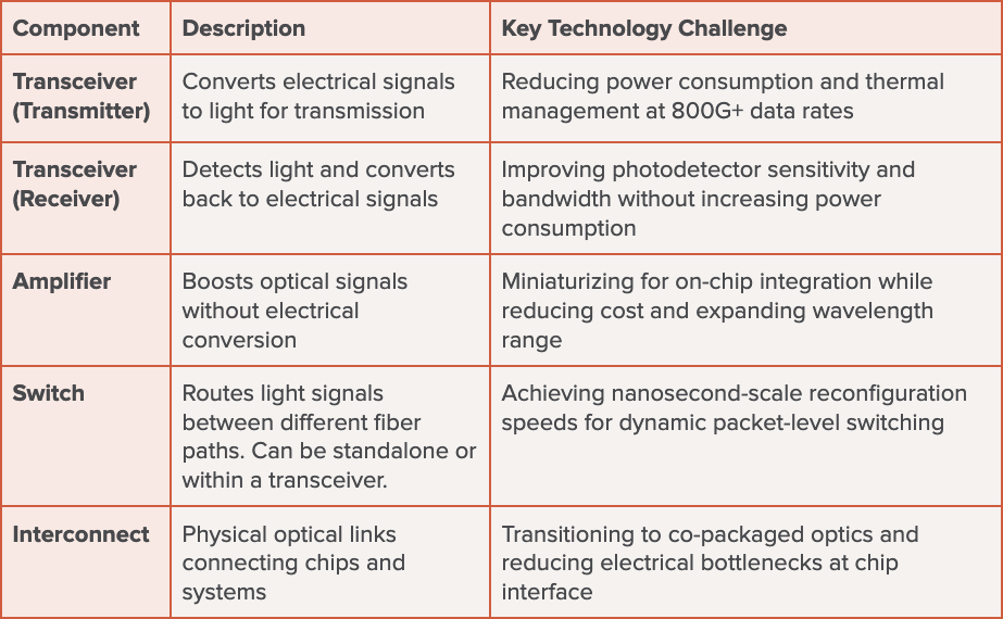
Table 1: Networking Components Summary
These networking innovations are not isolated. They feed directly into the next level of integration, co-packaged optics, and set the foundation for more ambitious photonic computing architectures.
Silicon Photonics and Materials Innovation
Silicon photonics (SiPh) has become the default platform for integrating photonic components such as modulators, waveguides, and detectors on a silicon wafer. The appeal is straightforward: leverage existing semiconductor processes, ride foundry learning curves, and co-locate optics with CMOS logic.
However, silicon has real limitations: higher optical losses and bandwidth constraints for certain functions. This has driven a wave of heterogeneous integration efforts that bring new materials into the photonics stack, including:
Silicon nitride (SiN) for lower-loss passive waveguides and non-linear optics.
III-V semiconductors like indium phosphide or quantum dot structures for better on-chip lasers and detectors.
Specialty oxides and other materials for integrated amplifiers and more efficient light generation.
From an investment perspective, these platforms often follow a familiar playbook: build on existing foundry processes, sample early devices, win design slots, then scale. The problem is that pure component businesses are brutally competitive, and what starts as a differentiated device can become a commodity as incumbents catch up.
The companies that tend to build more durable value are the ones that:
Use materials innovation to unlock performance that is otherwise unreachable.
Tie those components to clear system-level advantages, not just incremental specs.
Position themselves around standards or architectures that others must follow.
Electro-Optic Materials: Inorganics vs Organics
A key lever in high-speed photonics is how efficiently we can modulate light with an electrical signal. Electro-optic (EO) materials that exploit the Pockels effect (modulating light through applied electric fields) enable faster, lower-voltage modulation than silicon alone, which relies on less efficient mechanisms.
Inorganic platforms such as lithium niobate (LN) and barium titanate (BT) have strong physical properties and a long history in telecom and specialty applications. Thin-film variants and new epitaxy approaches are improving their performance and integration, and there is active work in Europe and elsewhere to build out dedicated manufacturing capacity. However, they still face issues around device size, integration with silicon electronics, contamination concerns, and the need for specialized foundries.
Organic EO materials take a different path. By achieving much higher electro-optic coefficients, they promise:
Lower drive voltages and smaller footprints.
Easier integration with standard silicon photonics processes and existing OSAT workflows.
Recent progress has focused on stability: passing demanding temperature and humidity tests, surviving solder reflow conditions, and avoiding long-term degradation. With these hurdles being addressed, some organic EO platforms now combine compelling performance with cleaner manufacturing stories that align better with mainstream high-volume fabs.
From a venture lens, the white paper’s conclusion is measured: inorganic materials may continue to play important roles in quantum, sensing, and imaging, but organics look more promising for mass-market EO conversion if capital requirements and valuations remain grounded.
Co-Packaged Optics: System-Level Integration Becomes the Battleground
Co-packaged optics (CPO) moves optics from the front panel into the package alongside compute and memory, reducing electrical bottlenecks and bringing light closer to where data is generated and consumed.
This is not just about plugging in faster transceivers. CPO requires:
Advanced packaging technologies that integrate photonic and electronic chiplets on a common substrate.
New control, diagnostics, and signal-processing capabilities to keep complex optical fabrics stable in real time.
Architectural shifts such as pooled memory, which decouples compute from memory capacity to address the “memory wall” in AI accelerators.
Market interest has surged. Large acquisitions and late-stage financings have validated the opportunity, and major incumbents in networking and compute are now building or buying their own platforms. At the same time, this success is raising the bar for new entrants: many of the most strategic technology slots are being filled, and future outcomes are unlikely to match the richest valuations seen so far unless they come with clear revenue traction and hyperscale commitments.
For LPs, CPO sits at the intersection of packaging, photonics, and AI infrastructure. It could become a very large business, but it is also becoming crowded, and differentiation increasingly depends on system architecture and customer adoption, not just device-level specs.
Photonic Computing: High Risk, Long Horizon
Photonic computing has promised step changes in bandwidth and energy efficiency by performing certain operations, like matrix multiplications, directly in the optical domain. In practice, several ambitious efforts have faced technical hurdles and pivots, especially around device size, programmability, and integration into existing software and hardware ecosystems.
A second wave of companies is taking a more focused approach:
Targeting specific computational bottlenecks such as optimization problems, encrypted computation, or niche AI inference workloads.
Combining photonics with mature material sets or waveguide platforms to keep manufacturing risk manageable.
Leveraging strong government funding, particularly in Europe, to tackle longer-horizon R&D without relying solely on venture capital.
The analogy to quantum computing is helpful. The most credible photonic computing concepts are not trying to replace general-purpose processors wholesale. Instead, they aim to excel at well-defined functions that are extremely expensive or slow on traditional architectures.
This is not a space for impatient capital. But for LPs comfortable with higher technical risk and longer time horizons, often via specialized funds, selective exposure can make sense as part of a broader computing infrastructure strategy.
Venture Perspective: What LPs Should Look For
Photonics has moved from the periphery of venture portfolios to the center of many AI-era hardware theses, driven by both genuine need and fear of missing out. Yet, as with most hard tech, enthusiasm alone does not build sustainable companies. The white paper highlights several patterns that tend to correlate with success:
Start with a sharp niche. Winning early often means solving a very specific, urgent problem, whether in data centers, networking, or a related domain, rather than going head-to-head in the largest, most entrenched markets first.
Leverage existing fabs and supply chains. Building a new foundry or highly specialized line is rarely compatible with the venture model. The strongest photonics companies find ways to fit into existing manufacturing infrastructure and OSAT processes.
Choose partners that actually move the needle. Not all partnerships are created equal. Deep engagement with leading customers or ecosystem players is far more valuable than a long list of minor collaborations. A thoughtful path to potential strategic acquisition can also be important in this sector.
Think at the system level when possible. Many innovations begin at the materials or component level, but the most durable platforms find ways to influence system architecture and industry roadmaps, not just slot into them.
Back teams with real domain depth. In a space that blends materials science, device physics, packaging, and semiconductor economics, management teams with relevant experience and relationships are critical.
Regulatory risk is real. Photonics are treated as critical and often defense-related technologies, so major acquisitions or strategic investments in U.S.-based companies can face intense regulatory scrutiny and geopolitical risk at exit.
Ultimately, photonics startups that combine differentiated technology, realistic manufacturing strategies, and credible system-level relevance are the ones most likely to generate venture-scale outcomes.
Insight for Japanese Corporate LPs
Japan has long been a leader in semiconductors, networking equipment, and precision manufacturing, and its companies sit close to the global supply chains underpinning AI infrastructure. As data centers scale and domestic demand for AI services grows, the need for high-bandwidth, energy-efficient interconnects and advanced packaging will only increase.
For Japanese corporates with a global innovation lens, photonics offers several angles: strategic adoption in domestic data centers and networks, partnerships with international startups to co-develop or localize key technologies, and selective LP or co-investment roles in funds that specialize in the most critical layers of the photonic stack. The most compelling start-up opportunities may not be headquartered in Japan, but they can still be deeply relevant to Japan’s future compute and networking landscape.
Photonics at the Edge of the Hard Tech Revolution
Photonics is no longer just the backbone of long-haul telecom. It is becoming a foundational layer for AI-era computing and networking, from data center interconnects and co-packaged optics to emerging photonic computing concepts. For LPs, and particularly for strategic investors in markets like Japan, where reliability, efficiency, and industrial competitiveness matter deeply, careful exposure to photonic innovation is increasingly part of participating in the hard tech revolution, not just watching it from the sidelines.